The TileSystem is the required flexible and compact embedded processing platform.
The concept was finalized during the MARISense project.
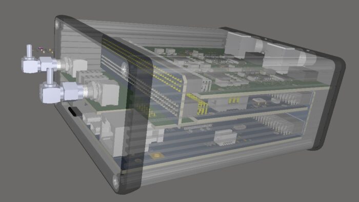
TileCube System
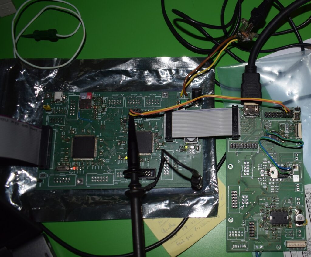
When all the parts of the system came, we were able to check the designed mechanical integration of a multi-board design using the Altium Designer CAD against the actual hardware. Initially, each component was checked that fit properly the mechanical enclosure. This was a preliminary test to verify PCB width and component height that might affect the assembly. Although the backplane boards are missing from the below setup, the HAT and other connectors and protruding pins were checked for potential conflicts.
4-Channel Hydrophone Edge Processing System
Then we added the back/front plane boards to complete and final check the system assembly.
The next step of the TileFPGA testing is the SDRAM interface.
As you may see in the following video, writing to the SDRAM memory space seems successful, but reading back the data by refreshing the debugger view, shows that the memory is sparsely written (or ghost read).
FPGA SDRAM Failed Access
This usually is an indicator of the clock phase, which can be addressed in the design’s clock generation phase. By adjusting the clock phase, the clock becomes in sync with the signals and hence the SDRAM is operating properly.
This concludes the TileFPGA testing for now. In the next blog the Hydro4 ADC interface will be checked.
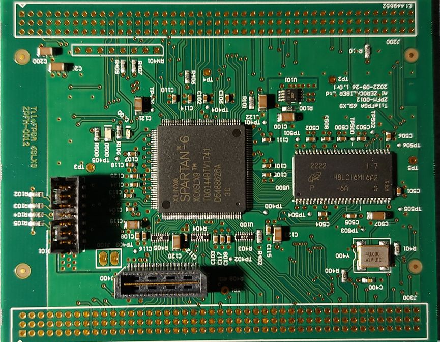
The second element of the TileSystem useful for edge processing is the FPGA board. This board interfaces tightly with the microcontroller of the system using a bus and also with the potential frontends for input or output.
As FPGAs are also hit by the component shortages in the semiconductor market, the design was based on AMD/Xilinx Spartan 6LX9 device, as this was in stock. The fact that the device is in a QFP package (as opposed to BGA) allows a less expensive PCB design with easier debugging, as all pins can be probed.
TileFPGA Board
The board was designed in less than 2 weeks and it came into our lab for verification. In order to test the board, we must connect it to our TileMCU through a backplane, and run the appropriate firmware that will load a valid configuration to the chip. A suitable test design with proper pin constraints was created.
After the assembly of the missing parts, the TileCUBE assembled with the microcontroller and the FPGA.
TileFPGA in Unconfigured State
The initial power-up lit our default LEDs (orange LED lit, means that the FPGA is unconfigured). We had to compile a test design with the updated pin-out from the Perseus CFE board to the TileFPGA. The design was placed at the SDCard. The firmware was adjusted to load this FPGA bitstream, so we can test the MCU and SDRAM interfaces.
FPGA in Configured State
After the FPGA was configured, we tested the Mini-FlexBus interface. We used the debugger to inspect the register area and confirmed the visibility (read operations). Registers were also written to verify that the interface is working as expected. We tested the LED state change (green color seen in the above photo) by changing the relevant bit in a register.
The next phase was to test the internal Block-RAMs. Initially the internal logic did not route the memories to the FlexBus interface (this was a design feature). the values seen in the memory space are 0xFFFF (due to the pull-ups inside the FPGA logic).
Block-RAM Access Enable and Test
Setting the respective enable bit in the control register the memory space can be written and the values are retained. Note that the default memory values seen by the Bus are 0xFFFF, but as soon as we step an instruction after the memory enable bit is set, the debugger refreshes the memory contents that are now zero.
These tests concluded the basic Mini-FlexBus interface and the internal Block-RAM interfaces. In the next post, we will test the SDRAM.
The TileMCU Coldfire version completed its first set of tests, completing the integration of the USB stack from Freescale/NXP to the RTOS.
Using POSIX-style drivers (or any standard way of interfacing) we were able to replace the Serial input of the Command Line Interpreter (CLI) with the USB one.
The code change was a very simple one, replacing just the name of the driver.
Code Excerpt of Selectable Driver
So essentially we define a preprocessor macro with the name of the required driver. As both the USB-CDC and the Serial driver have the same API, they can be interchanged at will.
Here we do this on compile time. Another option would be to mirror both interfaces and have at the same time either USB or Serial I/O. For now, we decided to keep it simple as we have to test the rest of the boards to complete our hydrophone system.
USB Enumeration
At first, the USB enumeration was checked to see if the basics worked. Then we opened with our terminal the respective virtual serial port and start testing the CLI.
CLI Test Example
The CLI was tested to ensure that there were no problems using it and testing some other functions like the SD Card mounting and FAT access.
As we have completed the first phase of testing we can move on to the next boards for testing. We will return back to this board to test the Mini-FlexBus interface with the FPGA.
The concept of a flexible and scalable system is a usual requirement for many applications. We initially started this flexibility by integrating MCUs with FPGAs on the same board. These created the initial Perseus Family Platform boards that we used for the development of applications.
Later on, during the MARI-Sense project, it was evident that the form factor should be more compact while features should be more selectable. In that spirit, we created the TileCubeTM System. Toward implementation of the platform, we designed boards for a complete hydrophone system, including microcontroller boards, FPGAs, and analog front-ends.
Due to component shortages, we were forced to design and use existing parts that we had in stock for the boards. Some boards are already designed with higher-performance microcontrollers waiting to have the new parts in hand. The flexibility of the system allows using different MCU boards in a backward-compatible manner.
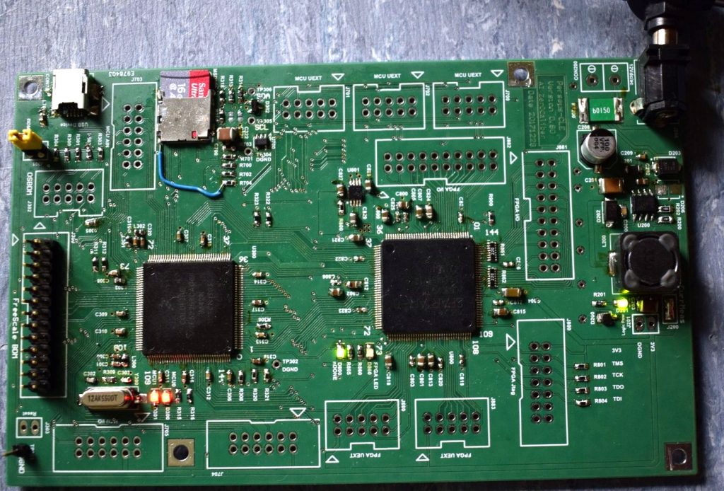
The first board of the Tile System is the microcontroller. This version is based on Coldfire MCF52258.
CAD Model of TileMCU_CF
Soon the boards arrived to our lab and we started the board bring-up process and testing.
Actual TileMCU_CF Sample
We confirmed the firmware configuration changes to support the new I/O assignment and installed COFILOS to test the system. Soon we had a system working with serial communications, command line interface (CLI), etc.
First Light (Blinking) of Firmware
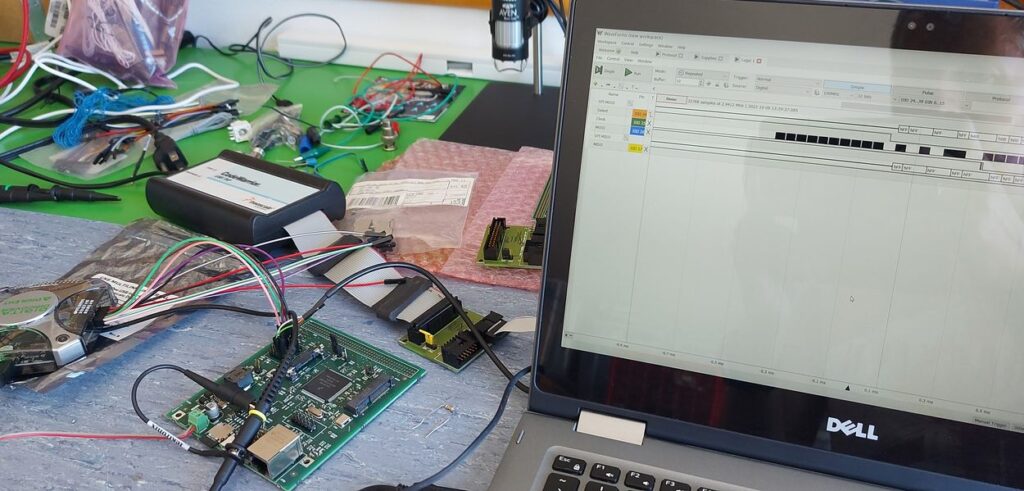
Next steps were to verify the SDCard interface and we tried the first time the Digilent Digital Discovery tool for capturing SPI data.
SDCard SPI Checks
Finally, we confirmed the proper operation of the SDCard and through the CLI we sneaked into the first sector of the device.
SDCard First Sector
Initially, the same board was designed with another microcontroller in mind, but due to component shortages, we had to re-spin the board with Coldfire. It was a fast race to quickly redesign the board, build it and make it work, within our deadlines. This gave us the motivation to complete the rest of the boards with the same speed, so we can see the full system ready and explore the potential of the system.
If you are interested in this platform feel free to contact us.
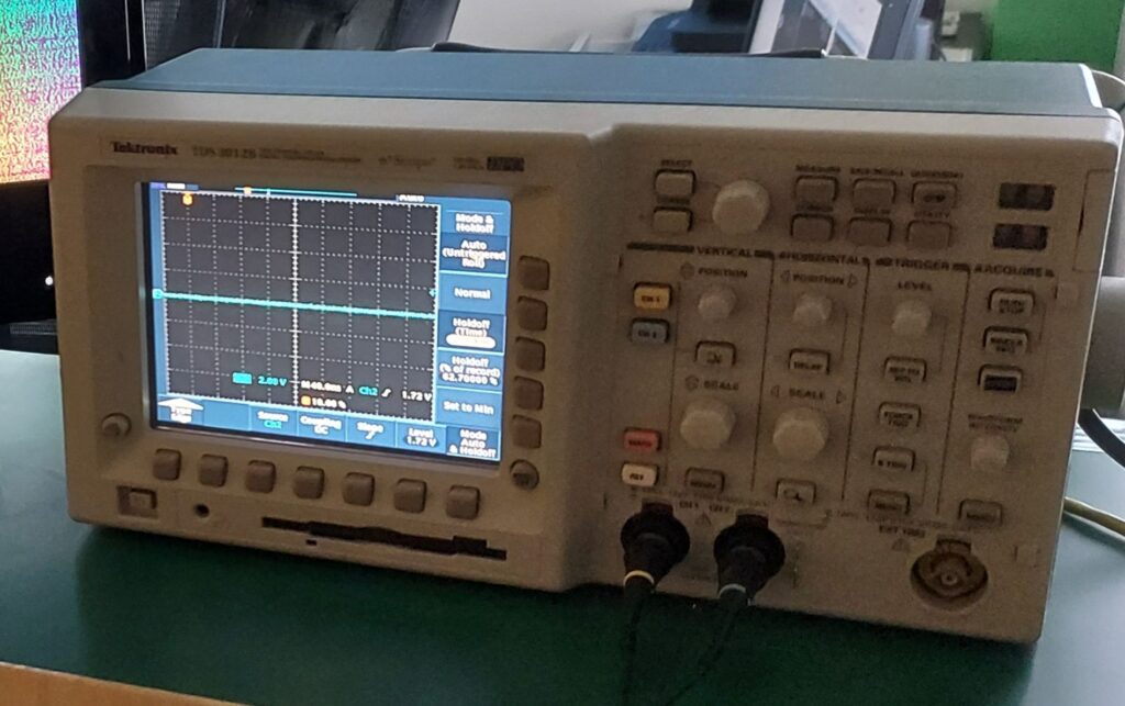
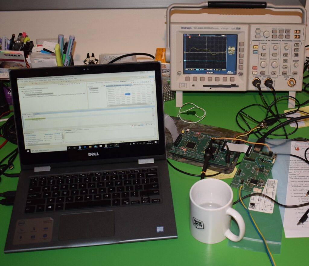
In the past 18 years I have been using a 100MHz two channel oscilloscope TDS3012B from Tektronix, which was using the new at the time Digital Phosphor technology (DPO). With a bandwidth of 100MHz back then it was sufficient for embedded design and debugging. I was missing the serial decode capabilities, but I was able to program a Python script for this purpose. For more information see my article in CodeProject.
Debugging a system with Atmel AVR and Xilinx Spartan (5K gates) device
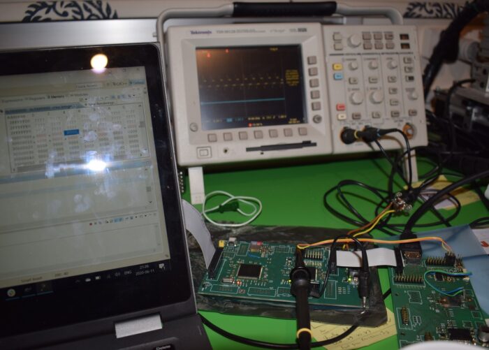
Back then it served me very well, although in some cases I would like to have four channels to help me resolve some problems. Not a showstopper anyway, I have been used to have less than ideal equipment. Recently the ethernet interface failed and this reduced the capabilities of my old instrument. In addition, my newer embedded boards started using SDRAMs or HDMI and the signal bandwidth of the scope was below my debugging needs. I had to guess the clock phase on my FPGA-SDRAM interface looking to sinewaves on my scope and trying an educated guess for the correct PLL phase delay. Fortunately, the first guess for the phase difference was correct, so this went smooth and my SDRAM worked fine without much hassle. The old floppy also prohibited data transfers or firmware updates.
According to Altium Designer research about new PCB designs, the trend is to go to boards with 500MHz. Although this might seem a little high for microcontrollers, I started feeling the pressure to go above 100MHz and for some newer serial protocols even higher. I had a SDRAM 133MHZ, but DDR starts to be more mainstream even for embedded systems. Purchasing a scope is an investment for the next 10 years and hence the capabilities should match at a great extent the future requirements. If we go to platform FPGA boards, like Ultra96 or PynQ, there are serial interfaces that can achieve clock frequencies above the 100MHz limit. So, I thought that my next scope should be certainly at the range of 350MHz. So, I decided to move on to a new scope like the MSO44 from Tektronix. A big thanks to Vector Technologies which helped me with my decision. In the next paragraphs, I will present some of the features from my preliminary tests of the new instrument. I still keep my TDS3012B around, as a secondary instrument for field work.
Last days of my TDS3012B Sitting on my lab, while expecting the MSO44.
Thank you TDS3012B for your service all these years!!
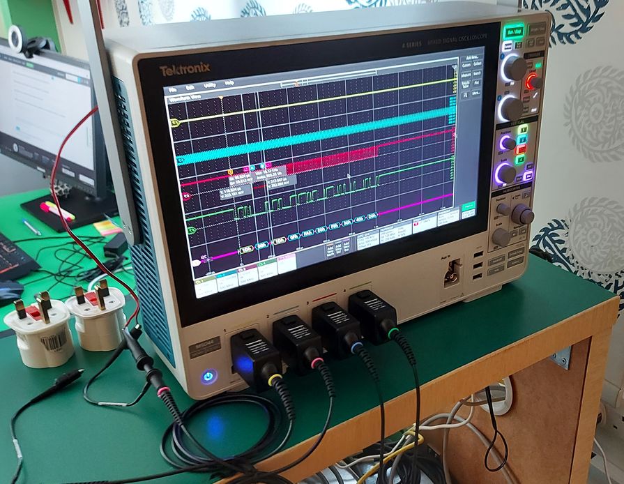
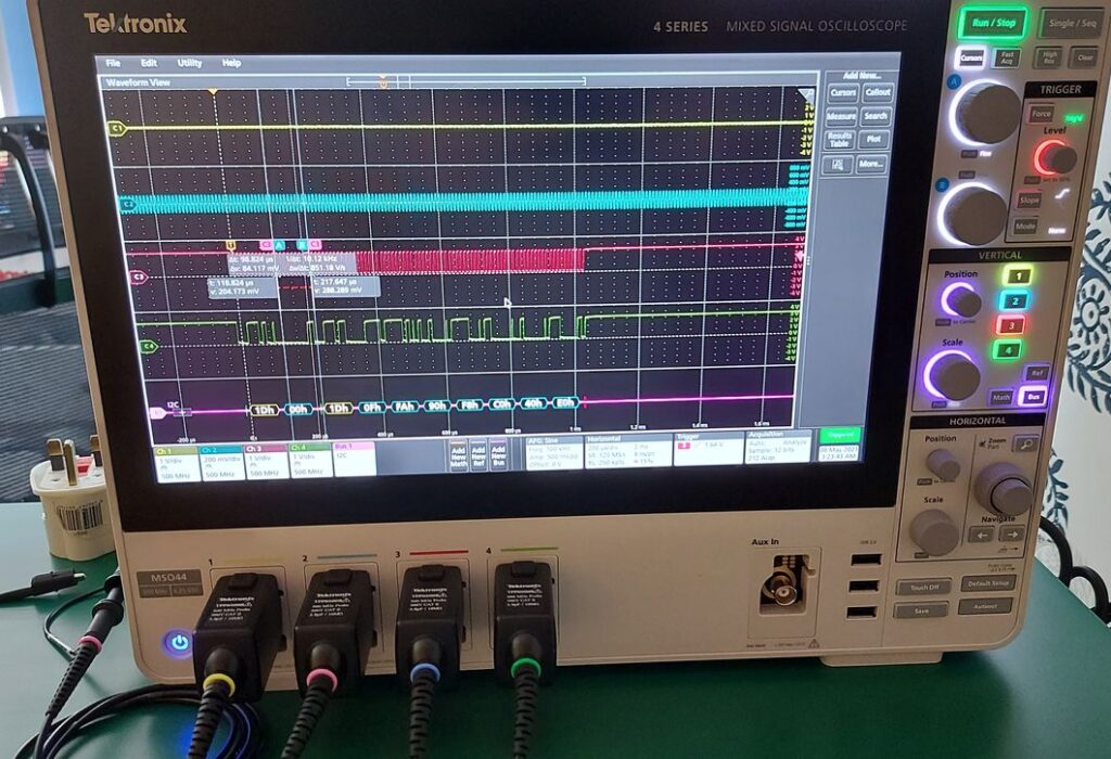
MSO44
The new instrument has four analog channels. This alone is an important upgrade. I can check full SPI bus with enables and clocks or combination of analog and digital lines on my board. A rarely used more than 4 channels unless I had to deal with a digital parallel bus. Even then looking at some control signals and one of the data could give you an idea of the situation. Nevertheless, an analog probe can be replaced by a digital counterpart with 8-channels digital inputs and used as a logic analyzer. You lose one analog channel for this, but it is a reasonable compromise. Other vendors provide this functionality without the analog probe loss, but I do not believe or remember a case in the past that this would be an issue.
A quick view of the MSO44 in action
The next major upgrade is the bandwidth of 500MHz. Hey, I can check my SDRAM clock easily now… I want to check at some point my HDMI signals (at 250MHz). The 500MHz though can be used also for RF applications at 433MHz, through the spectrum analyzer feature. Really neat.
The arbitrary function generator feature is really useful as with one instrument I can also exercise my circuits. I plan to use this feature for testing the Hydrophone Analog Front End and the FPGA data capture.
I am not going to stay at the UI features most instruments in this category have recently, the large touchscreen etc. Having a large screen estate is important to view multiple signals.
One important aspect of the new generation of instruments is that they offer upgrades by license. So, you can upgrade the bandwidth or some features (more serial busses decoding etc) by purchasing them later according to your needs or projects. This provides a more viable solution where you start with some specific requirements and you can scale up the instrument according to your needs later-on.
Serial Decode
The instrument supports serial decoding of common protocols like RS232, I2C or SPI. This is useful for debugging peripherals or components to your microcontroller. To test this feature I tried an I2C interface on one of my boards. The abundance of screen area is useful to put all the signals without too much clutter and in addition have the serial bus decoding.
Serial Bus decode of an I2C bus
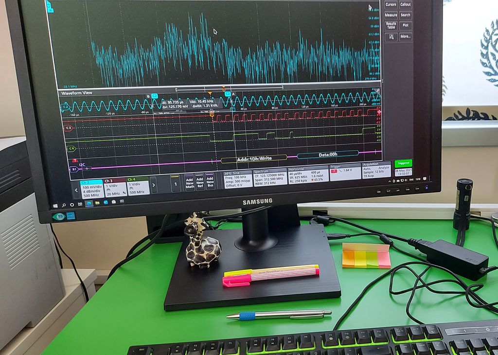
Web Interface
Connectivity is important, so the instrument comes with a bunch of USB ports and an ethernet port for network. This is what I used with a web browser to mirror my MSO screen to my desktop PC. Extremely helpful if you want to control the instrument from the same place as you control your debugger. No need to turn your chair around to turn knobs.
MSO screen view on my desktop PC
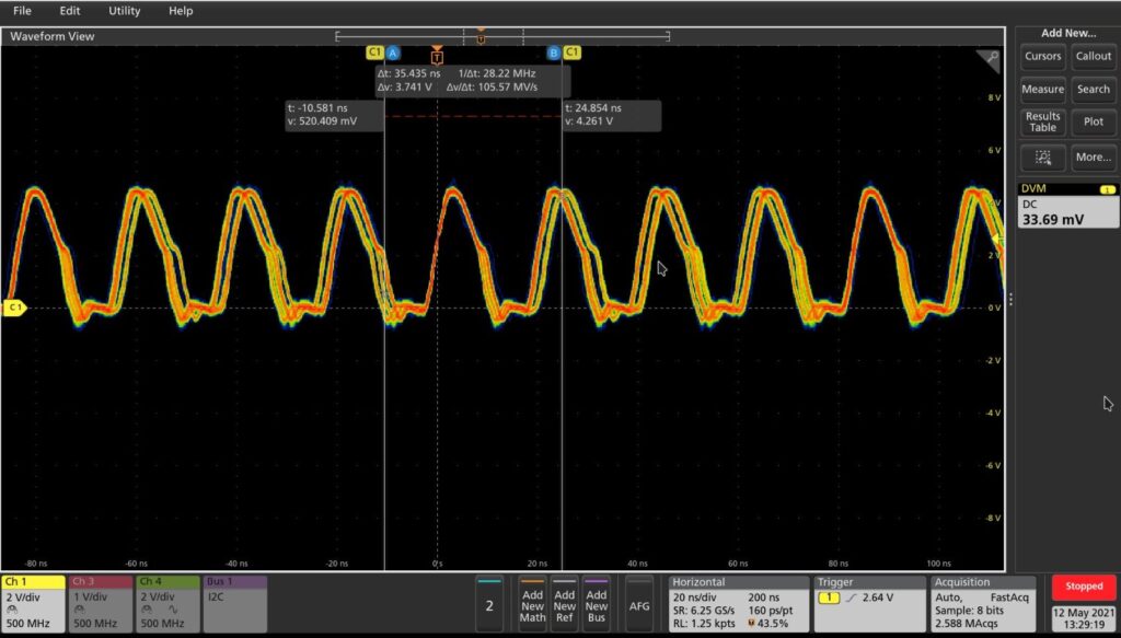
Jitter Tests
On one of my boards, I knew that there is some jitter on my clock. So, I decided to test the DPO capabilities and look in more detail on this signal. I can see the probability of states clearly. I want to delve more on this feature in the future.
Clock Jitter seen through DPO
Spectrum Analyzer
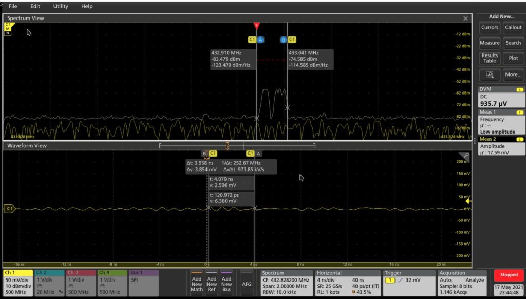
Yes, many engineers would say that this is the FFT button or feature found on most of the scopes, so what’s the big deal. Well, nope. The FFT feature exists in the math menu and is not the same with the spectrum analyzer feature, which works like a spectrum analyzer. I mean you need to setup video bandwidth, resolution bandwidth and so on, as you would do in an actual spectrum analyzer. In addition, changing the time domain signal (scaling-resolution) does not affect the spectrum and vice-versa. I read about this feature on the website when looking at the specifications and I was keen to see it in action. Having worked with spectrum analyzers in the past, I got pretty familiar with the parameters. This feature exists inside the channel settings (tap on your channel and select spectrum tab). Testing this feature, I tried a remote of 433MHz. The probe was attached at the antenna signal on the receiver side.
Spectrum of a remote at 433MHz
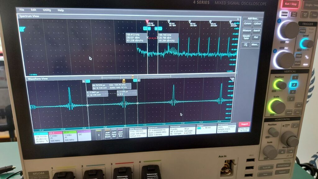
I even went further. I have some LoRa devices working at 433MHz and wanted to confirm that this is their center frequency. As LoRa uses broadband transmission, I set-up my instrument to capture and hold the maximum level. So after a while transmitting, the spectrum started to show activity, by filling bands.
Spectrum max hold at 433MHz, LoRa transmission
Arbitrary Function Generator
Providing stimulus to your circuits is essential when designing and testing analog to digital converters. Applying some basic stimulus may help you check design elements and ensure that the basics work. For more thorough testing you will need a dedicated instrument. In this case the arbitrary function generator is used for the first line of defense. Here a sinc function is output and its spectrum is displayed.
Arbitrary Function Generator and Spectrum
Conclusion
I will need to spend lots of time to test every aspect of the new instrument. I am already using it in my projects, and I am getting used to it. Albeit the complexity of the functions, I can navigate around, put the right settings without hassle, giving me time and insight and let me be productive. I have a long queue of things that needs development and testing that this instrument will help me a lot.
Our laboratory is now massively upgraded and ready to win the next battles!
Some time ago I wanted to test the capabilities of the PerseusCLE board. I created an expansion card which supported motor drivers for DC Brushed or Stepper motors, Analog front ends etc.
I always wanted to try and output a DVI/HDMI signal using TMDS and I knew that my spartan 6 device was capable of doing this. However when I initially designed PerseusCLE, I did not think at all trying this, I just wanted a strip-down version of my bulky PerseusCFE to a more cost effective solution.
What are these CLE/CFE stand for anyway? Well I started with CFE: Coldfire Full Edition.
Perseus CFE Board
This board had all the bells and whistles I wanted at the time. Dual switching power supplies (logic and motor power), second crystal for the FPGA clock, SDRAM on FPGA, Ethernet connectivity, USB connectivity, SD Card, CANBus, model servo PWM outputs and lot’s of Olimex UEXT connectors for UEXT modules. All in just 2 layers PCB.
The board is large and I wanted something smaller and cheaper. Hence I decided to strip down many of the features of the Full Edition, creating the CLE: Coldfire Light Edition.
Perseus CLE Board
Features reduced to a minimum, like SDCard, native USB only, no separate FPGA clock (used same clock as MCU), still many connectors and a single switching power supply.
So designing the expansion board, I thought to give it a try and add an HDMI connector with a crystal oscillator to provide the missing external clock to my FPGA. I tried to match signal length for the TMDS signals from the FPGA to the expansion board as initially did not plan to have equal signal lengths up to the PerseusCLE connectors. It wasn’t my intention to drive so high speed signals back then. I needed to use Excel and measuring the length on the main board and calculating what was the actual signal length for each signal and add the corresponding missing length in the I/O board. Pretty challenging.
You can find how DVI/HDMI works as a concept and a Verilog implementation at FPGA4FUN. However I am using VHDL and searching the net I found various implementations some from Xilinx some from derivative works of Mike Field. I used a mix of the available sources. I liked this repo from drxzc. I also created and tested with GHDL Xilinx IP, like PLL and SERDES modules.
I was so anxious that I procrastinated to check the actual hardware. After creating the interconnections and verified that the setup was probably good, I decided to give it a try.
Perseus CLE and DVI Expansion
Although I expected to fail, I hoped for the best. Everything was wrong. The TMDS signals had to pass a simple flat cable to interconnect the boards. My reference 25MHz clock had to go with wires back to the main board. In order to reduce the effects of the signal integrity, I used a low resolution of 640×480. For simplicity I added a simple pattern generation. The idea if this worked was to replace it with video memory that the microcontroller would write. The bit rate in the data lanes would be 10 times my 25MHz clock giving 250Mbps per lane. This is where the TV shows says: “Don’t do this at home, experiment executed by Experts”. Well I would stick on the first part: “Don’t do this at home”; I see no expert around….
I put my FPGA configuration to my SDCard and modified COFILOS code to load this DVI configuration. I checked that my reference clock was running. My poor 100MHz DPO had not a good chance to capture the high speed data lanes of the serializers outputs.
DVI Test Setup
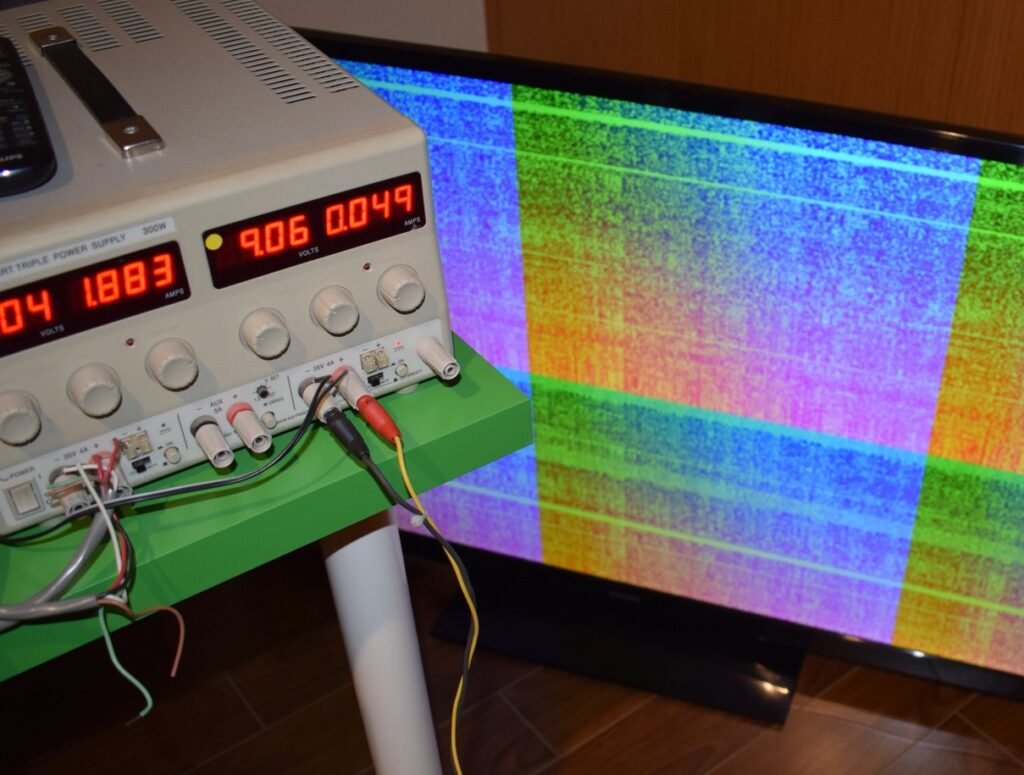
When my full setup was up an running I connected the HDMI cable… Silence. Excitement. Fear. Waiting to see the result. Nope, needed to select the correct HDMI input at the television. Ok. Let’s see. Oh!
My test monitor with the noisy test pattern on it
It worked! Well not as it should, but given the circumstances and the implementation I had to follow I am more than happy. The next boards would be tailored to provide proper signal integrity and produce a clean signal.
I did a small redesign in my VHDL to make sure that the issue I was looking, was not related to internal FPGA timings, instead of driving with my test pattern generator I tried driving a constant RGB value. Retrying this on another monitor I had very similar results. I need more specialized hardware to drive it with proper signal integrity and clock signals. No surprise.
At a later time, I also tried to use the internal PLL to generate my clock frequencies. I was not happy with my external 25MHz clock running around. I also did some modifications on my VHDL code as follows .
First I created generics input for the various VESA timings. Now the design is parametric. I also changed the color values to be zero during sync. To reduce timing issues on place and route I also used registered outputs from the Test Pattern Generator.
I started the experiments again with either clock coming from my MCU and create the clock frequencies using the PLL, but still got same results.
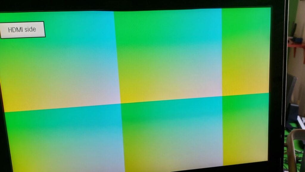
DVI Setup, 2nd try
As this setup had the same behavior as the original configuration, I reverted to the external 25MHz clock. It seems that this worked after the last changes! I had my DVI output on my monitor. Sometimes tweaking with the HDMI cable could lose the stability of my signal, or maybe the stability of my clock signal going around with cables was not good enough to have a good output, but nevertheless, the proof of concept was completed.
Working DVI pattern
It was really fun to work with SERDES and proprietary vendor IPs and see how they actually work. Really getting into these details provide a good background for other applications.