The second element of the TileSystem useful for edge processing is the FPGA board. This board interfaces tightly with the microcontroller of the system using a bus and also with the potential frontends for input or output.
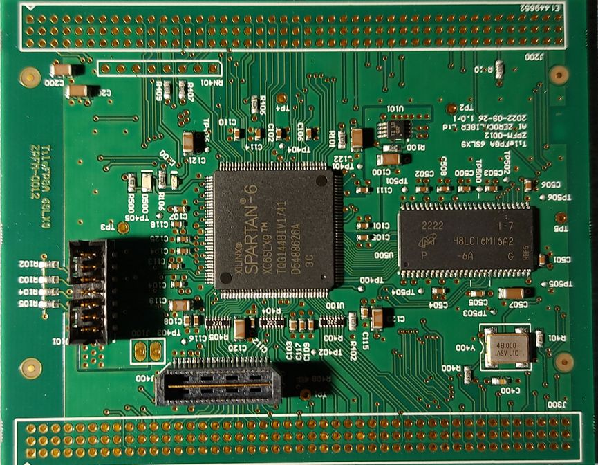
As FPGAs are also hit by the component shortages in the semiconductor market, the design was based on AMD/Xilinx Spartan 6LX9 device, as this was in stock. The fact that the device is in a QFP package (as opposed to BGA) allows a less expensive PCB design with easier debugging, as all pins can be probed.
TileFPGA Board
The board was designed in less than 2 weeks and it came into our lab for verification. In order to test the board, we must connect it to our TileMCU through a backplane, and run the appropriate firmware that will load a valid configuration to the chip. A suitable test design with proper pin constraints was created.
After the assembly of the missing parts, the TileCUBE assembled with the microcontroller and the FPGA.
TileFPGA in Unconfigured State
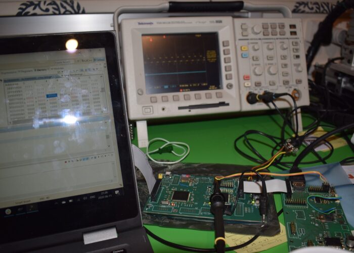
The initial power-up lit our default LEDs (orange LED lit, means that the FPGA is unconfigured). We had to compile a test design with the updated pin-out from the Perseus CFE board to the TileFPGA. The design was placed at the SDCard. The firmware was adjusted to load this FPGA bitstream, so we can test the MCU and SDRAM interfaces.
FPGA in Configured State
After the FPGA was configured, we tested the Mini-FlexBus interface. We used the debugger to inspect the register area and confirmed the visibility (read operations). Registers were also written to verify that the interface is working as expected. We tested the LED state change (green color seen in the above photo) by changing the relevant bit in a register.
The next phase was to test the internal Block-RAMs. Initially the internal logic did not route the memories to the FlexBus interface (this was a design feature). the values seen in the memory space are 0xFFFF (due to the pull-ups inside the FPGA logic).
Block-RAM Access Enable and Test
Setting the respective enable bit in the control register the memory space can be written and the values are retained. Note that the default memory values seen by the Bus are 0xFFFF, but as soon as we step an instruction after the memory enable bit is set, the debugger refreshes the memory contents that are now zero.
These tests concluded the basic Mini-FlexBus interface and the internal Block-RAM interfaces. In the next post, we will test the SDRAM.
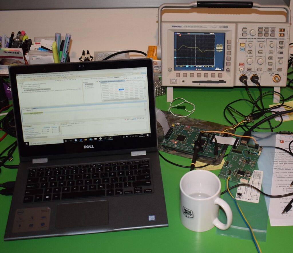
Some time ago I wanted to test the capabilities of the PerseusCLE board. I created an expansion card which supported motor drivers for DC Brushed or Stepper motors, Analog front ends etc.
I always wanted to try and output a DVI/HDMI signal using TMDS and I knew that my spartan 6 device was capable of doing this. However when I initially designed PerseusCLE, I did not think at all trying this, I just wanted a strip-down version of my bulky PerseusCFE to a more cost effective solution.
What are these CLE/CFE stand for anyway? Well I started with CFE: Coldfire Full Edition.
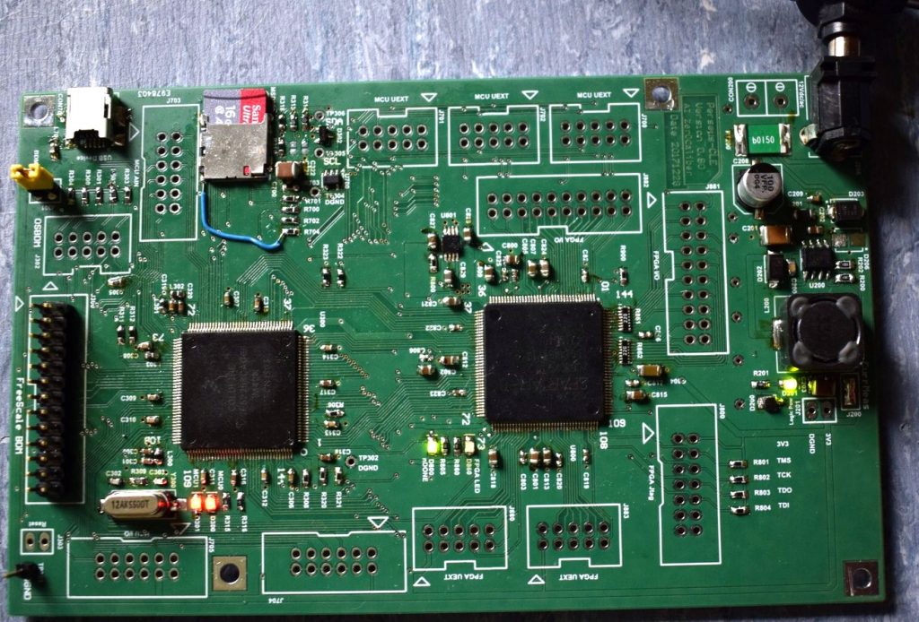
Perseus CFE Board
This board had all the bells and whistles I wanted at the time. Dual switching power supplies (logic and motor power), second crystal for the FPGA clock, SDRAM on FPGA, Ethernet connectivity, USB connectivity, SD Card, CANBus, model servo PWM outputs and lot’s of Olimex UEXT connectors for UEXT modules. All in just 2 layers PCB.
The board is large and I wanted something smaller and cheaper. Hence I decided to strip down many of the features of the Full Edition, creating the CLE: Coldfire Light Edition.
Perseus CLE Board
Features reduced to a minimum, like SDCard, native USB only, no separate FPGA clock (used same clock as MCU), still many connectors and a single switching power supply.
So designing the expansion board, I thought to give it a try and add an HDMI connector with a crystal oscillator to provide the missing external clock to my FPGA. I tried to match signal length for the TMDS signals from the FPGA to the expansion board as initially did not plan to have equal signal lengths up to the PerseusCLE connectors. It wasn’t my intention to drive so high speed signals back then. I needed to use Excel and measuring the length on the main board and calculating what was the actual signal length for each signal and add the corresponding missing length in the I/O board. Pretty challenging.
You can find how DVI/HDMI works as a concept and a Verilog implementation at FPGA4FUN. However I am using VHDL and searching the net I found various implementations some from Xilinx some from derivative works of Mike Field. I used a mix of the available sources. I liked this repo from drxzc. I also created and tested with GHDL Xilinx IP, like PLL and SERDES modules.
I was so anxious that I procrastinated to check the actual hardware. After creating the interconnections and verified that the setup was probably good, I decided to give it a try.
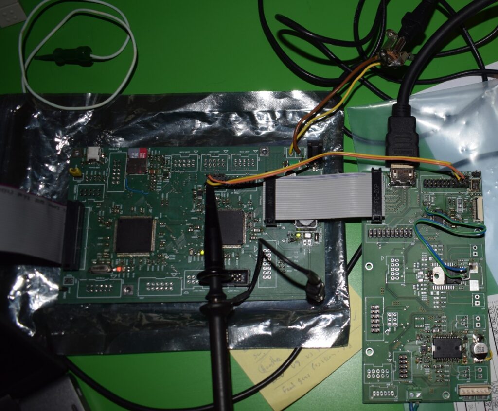
Perseus CLE and DVI Expansion
Although I expected to fail, I hoped for the best. Everything was wrong. The TMDS signals had to pass a simple flat cable to interconnect the boards. My reference 25MHz clock had to go with wires back to the main board. In order to reduce the effects of the signal integrity, I used a low resolution of 640×480. For simplicity I added a simple pattern generation. The idea if this worked was to replace it with video memory that the microcontroller would write. The bit rate in the data lanes would be 10 times my 25MHz clock giving 250Mbps per lane. This is where the TV shows says: “Don’t do this at home, experiment executed by Experts”. Well I would stick on the first part: “Don’t do this at home”; I see no expert around….
I put my FPGA configuration to my SDCard and modified COFILOS code to load this DVI configuration. I checked that my reference clock was running. My poor 100MHz DPO had not a good chance to capture the high speed data lanes of the serializers outputs.
DVI Test Setup
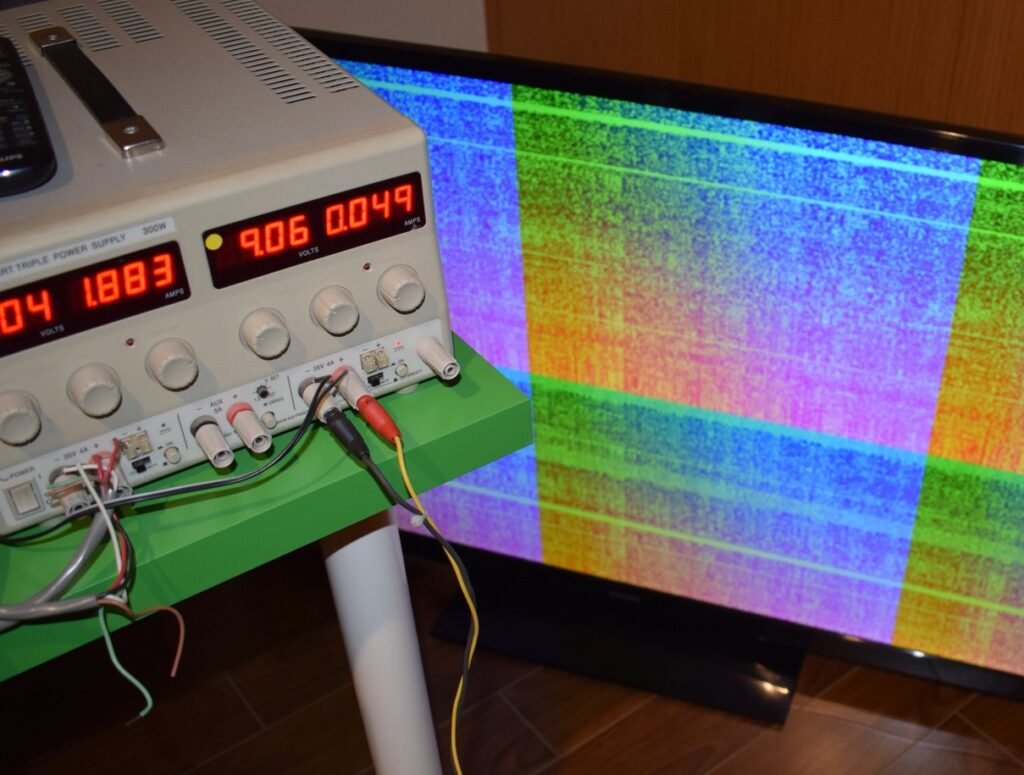
When my full setup was up an running I connected the HDMI cable… Silence. Excitement. Fear. Waiting to see the result. Nope, needed to select the correct HDMI input at the television. Ok. Let’s see. Oh!
My test monitor with the noisy test pattern on it
It worked! Well not as it should, but given the circumstances and the implementation I had to follow I am more than happy. The next boards would be tailored to provide proper signal integrity and produce a clean signal.
I did a small redesign in my VHDL to make sure that the issue I was looking, was not related to internal FPGA timings, instead of driving with my test pattern generator I tried driving a constant RGB value. Retrying this on another monitor I had very similar results. I need more specialized hardware to drive it with proper signal integrity and clock signals. No surprise.
At a later time, I also tried to use the internal PLL to generate my clock frequencies. I was not happy with my external 25MHz clock running around. I also did some modifications on my VHDL code as follows .
First I created generics input for the various VESA timings. Now the design is parametric. I also changed the color values to be zero during sync. To reduce timing issues on place and route I also used registered outputs from the Test Pattern Generator.
I started the experiments again with either clock coming from my MCU and create the clock frequencies using the PLL, but still got same results.
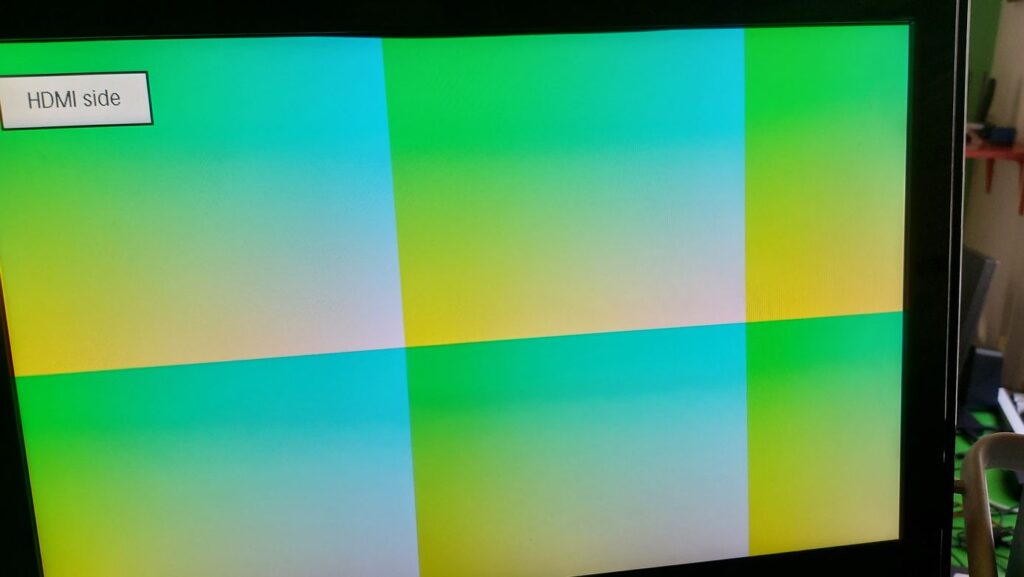
DVI Setup, 2nd try
As this setup had the same behavior as the original configuration, I reverted to the external 25MHz clock. It seems that this worked after the last changes! I had my DVI output on my monitor. Sometimes tweaking with the HDMI cable could lose the stability of my signal, or maybe the stability of my clock signal going around with cables was not good enough to have a good output, but nevertheless, the proof of concept was completed.
Working DVI pattern
It was really fun to work with SERDES and proprietary vendor IPs and see how they actually work. Really getting into these details provide a good background for other applications.
Hardware and Firmware development is essential for the age of the Internet of Things or the more traditional term embedded systems. Recently more and more processing is required to be performed closer at the physical locations where the sensory or IoT devices exist, called edge processing. The traditional way of developing such systems is using application processor systems running on Linux.
Development of such products is fast due to the ecosystem using commercially available platforms and proof of concept projects are easy to achieve; However when someone tries to make the necessary modifications to create a custom product, comply with certifications, and perform changes required to make it a viable product, soon he/she may fail short, as:
There is not much control for customizing the core boards; Design from scratch is the only option if a single board is needed or there are mechanical constraints
The base hardware is complicated for the majority of applications
Highly skilled hardware engineers and sophisticated tools are needed
Cost for the production of a custom-featured PCB usually is much higher for individual production
Critical parts are hard to source in small quantities
Designs may not be efficient from a power or performance perspective
We are often obliged to select and change parts because of the limitations of our mainstream microcontrollers to a higher-end one or we need to add external logic and circuits to accommodate richer input-output architecture.
Wouldn’t be great to have a polymorphic platform that could easily scale to work with for the majority of our projects, smaller or bigger?
Another aspect that is considered is design verification. Embedded systems usually need to have real-time performance, thus classic debugging (step-through) under real-time conditions is not always possible or is an additional challenge. Stack checking on RTOS or timings is not easy to observe accurately without the help of hardware otherwise, a performance penalty is taken.
Wouldn’t be great to have a much easier time debugging embedded systems?
our Solution
Microcontrollers offer a small footprint system with a high level of integration (memories, peripherals etc), but sometimes the internal peripherals or the processing capabilities are not adequate to tackle more demanding applications. FPGA on the other side is more flexible and capable but they are not the best option for control flows and require expertise for development. In addition edge processing often requires a higher processing capacity at a lower power rate.
We created a heterogeneous embedded platform with its firmware ecosystem, that allows fast application development, without compromising the later steps for final production. To combine the benefits of both microcontrollers and FPGAs the PerseusCLE was built.
This platform provides the following key features:
KeyFeatures
Simple 2 or 4-layer PCB, which is within a medium-skilled engineer to modify
32-bit microcontroller
Programmable Hardware to create custom peripherals and interfaces
A firmware framework that allows fast development in C language
A compact and extensible platform
Support of External Hardware parts for specific interfaces (motors, servos etc)
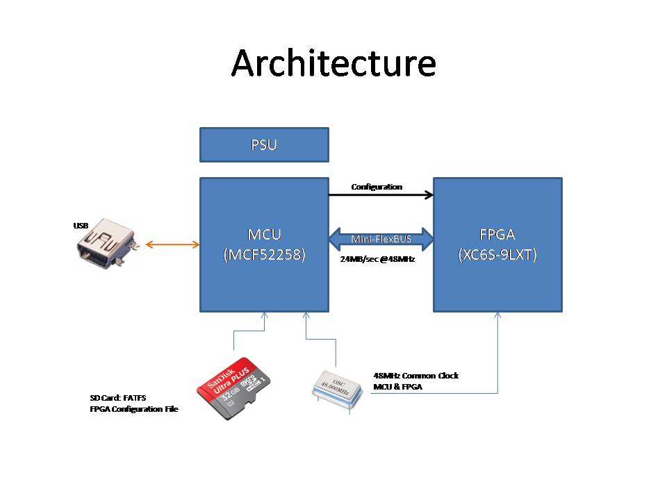
The two major parts (MCU, FPGA) are interlinked with a high-speed connection to enable FPGA mapping inside the microcontroller’s memory space, giving programming simplicity for the firmware, while achieving high-speed transfers and allowing the use of internal MCU DMA. Eventually, this provides a two-chip solution and simple two-layer PCB which allows low cost on low production quantities.
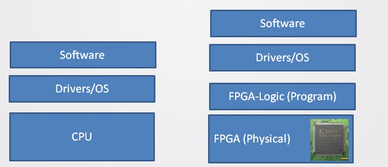
MCU vs FPGA Layer Stack Comparison
On the left side, we see the traditional CPU stack. If we upgrade the CPU we need to change the Driver/OS layer to fit the new CPU/Hardware
On the right side, the FPGA device is replaced. We need to “recompile” the FPGA-Logic (Program) to the new device. Driver/OS does not need to change! Using FPGAs moves the programmable barrier lower to the layer stack of a product.
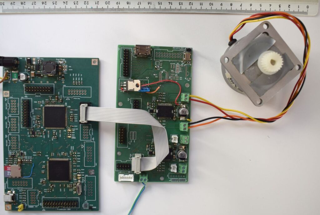
As an example, the flexibility of these platforms is demonstrated next, where the same platform can be used for DC motor control or drive an HDMI monitor, with the use of an adaptor board.
Stepper Motor FPGA DriveDVI SetupWorking DVI pattern
This example demonstrates how a core computing module can drive diverse applications, without requiring power-hungry complicated hardware (ie. high-end processors).
As not all applications require an FPGA, our next generation of embedded platforms is based on a scalable and flexible architecture in which additional elements can be added to the main microcontroller-based processing unit. The programmable hardware can provide one more level of expansion thus providing a more reach peripheral set than the ones included in of the shelf microcontrollers.
In the next picture, the design of a 2 channel hydrophone acquisition and processing system is shown. Note that the hydrophone analog front-end was a new requirement that the platform was not specifically addressed, which is managed to interface without any issues.
Hydrophone System
The hydrophone front-end is in the new form factor of the embedded tile, so it can fit on the mechanical chassis. The box offers a constant volume that can fit any combination of hardware in the same externally allocated space.
Applications
This platform can be used very effectively for the following
applications.
Embedded System for Hydrophone Processing with Chassis
Unmanned Vehicles
As the hardware is flexible, controlling multiple motors and acquiring sensor data from multiple sensors, make this platform ideal. The MCU can be off-loaded from low-level motor driving while concentrating on the main control system. The FPGA can handle the low-level functions along with the sensor fusion for multiple sources (ie. camera).
3D Printers
Having a platform that can handle more motors can create a more capable 3D printer or even a 3D printer in combination with a lathe. Again the high-level functions can run on the controller while the FPGA keeps track of the precision in time.
Small Video
Applications
The video signals stopped being analog and transformed into high-speed interfaces. The Spartan 6 series can handle these and create video input or output generators (or a combination thereof) while the microcontroller can handle the content (ie. transfer it through the USB). No more complex CPU high-frequency arrangements are required.
Edge Processing
As the FPGA can offer a high degree of parallelization, applications that require a high number of parallel units or hardware acceleration are good candidates for this platform. For example, this platform is going to be used in the MARI-Sense project for signal classification at the edge.
Embedded Design Verification For many applications the FPGA is an overkill device to have. However, you may be able to test the real-time embedded firmware, without any performance impact if you use the FPGA for capturing processor data. For example, stack checking in hardware is very efficient and accurate. So you can use the combined system to trace events, check stacks, and any other aspects of your embedded system before you deploy it and gain more confidence in the quality of your product.
Other
solutions
Well, why should I use this platform when I can get similar setups from the FPGA vendors? I can get single or dual ARM cores along with a larger set of available logic.
This is true, however, these solutions are micro-processor based and not micro-controller based. The PCB is challenging to accommodate these devices and they still need a lot of external peripherals to make it work (SDRAM, Flash etc). Our solution offers a two-chip solution (MCU and FPGA) that is more compact less power-hungry and within the design reach of a small or medium-sized company. In addition, the platforms are scalable.
What is the advantage of a microcontroller-based solution that contains logic?
Using an external FPGA device your solution is not bonded to a specific microcontroller or FPGA device. The split architecture allows more flexibility. You can scale up capacity for example using the same footprint (just replace the FPGA with a higher capacity logic one), or you may decide you need another processor (ie. Coldfire or Kinetis) that supports the same inter-chip interface.
Please contact us for further information on your heterogeneous embedded platform!