The second element of the TileSystem useful for edge processing is the FPGA board. This board interfaces tightly with the microcontroller of the system using a bus and also with the potential frontends for input or output.
As FPGAs are also hit by the component shortages in the semiconductor market, the design was based on AMD/Xilinx Spartan 6LX9 device, as this was in stock. The fact that the device is in a QFP package (as opposed to BGA) allows a less expensive PCB design with easier debugging, as all pins can be probed.
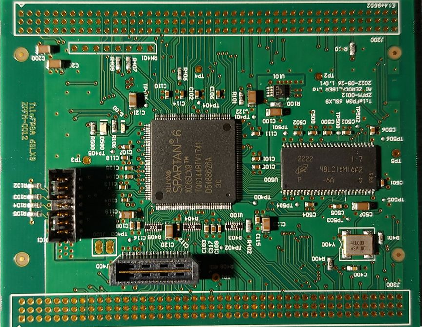
The board was designed in less than 2 weeks and it came into our lab for verification. In order to test the board, we must connect it to our TileMCU through a backplane, and run the appropriate firmware that will load a valid configuration to the chip. A suitable test design with proper pin constraints was created.
After the assembly of the missing parts, the TileCUBE assembled with the microcontroller and the FPGA.

The initial power-up lit our default LEDs (orange LED lit, means that the FPGA is unconfigured). We had to compile a test design with the updated pin-out from the Perseus CFE board to the TileFPGA. The design was placed at the SDCard. The firmware was adjusted to load this FPGA bitstream, so we can test the MCU and SDRAM interfaces.

After the FPGA was configured, we tested the Mini-FlexBus interface. We used the debugger to inspect the register area and confirmed the visibility (read operations). Registers were also written to verify that the interface is working as expected. We tested the LED state change (green color seen in the above photo) by changing the relevant bit in a register.
The next phase was to test the internal Block-RAMs. Initially the internal logic did not route the memories to the FlexBus interface (this was a design feature). the values seen in the memory space are 0xFFFF (due to the pull-ups inside the FPGA logic).
Setting the respective enable bit in the control register the memory space can be written and the values are retained. Note that the default memory values seen by the Bus are 0xFFFF, but as soon as we step an instruction after the memory enable bit is set, the debugger refreshes the memory contents that are now zero.
These tests concluded the basic Mini-FlexBus interface and the internal Block-RAM interfaces. In the next post, we will test the SDRAM.