Some time ago I wanted to test the capabilities of the PerseusCLE board. I created an expansion card which supported motor drivers for DC Brushed or Stepper motors, Analog front ends etc.
I always wanted to try and output a DVI/HDMI signal using TMDS and I knew that my spartan 6 device was capable of doing this. However when I initially designed PerseusCLE, I did not think at all trying this, I just wanted a strip-down version of my bulky PerseusCFE to a more cost effective solution.
What are these CLE/CFE stand for anyway? Well I started with CFE: Coldfire Full Edition.

This board had all the bells and whistles I wanted at the time. Dual switching power supplies (logic and motor power), second crystal for the FPGA clock, SDRAM on FPGA, Ethernet connectivity, USB connectivity, SD Card, CANBus, model servo PWM outputs and lot’s of Olimex UEXT connectors for UEXT modules. All in just 2 layers PCB.
The board is large and I wanted something smaller and cheaper. Hence I decided to strip down many of the features of the Full Edition, creating the CLE: Coldfire Light Edition.
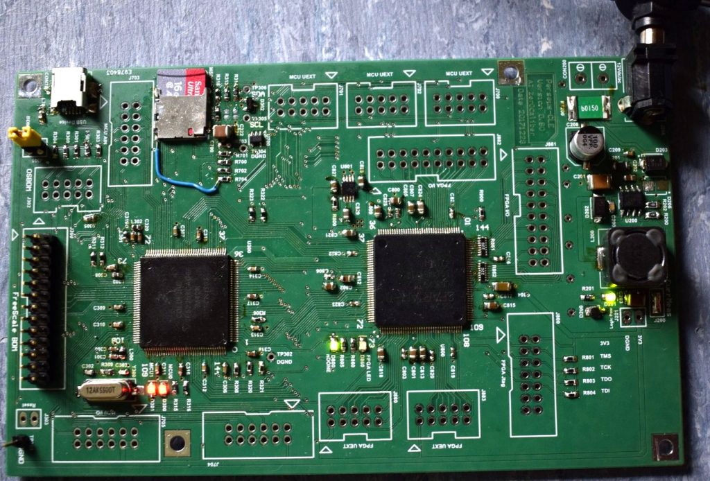
Features reduced to a minimum, like SDCard, native USB only, no separate FPGA clock (used same clock as MCU), still many connectors and a single switching power supply.
So designing the expansion board, I thought to give it a try and add an HDMI connector with a crystal oscillator to provide the missing external clock to my FPGA. I tried to match signal length for the TMDS signals from the FPGA to the expansion board as initially did not plan to have equal signal lengths up to the PerseusCLE connectors. It wasn’t my intention to drive so high speed signals back then. I needed to use Excel and measuring the length on the main board and calculating what was the actual signal length for each signal and add the corresponding missing length in the I/O board. Pretty challenging.
You can find how DVI/HDMI works as a concept and a Verilog implementation at FPGA4FUN. However I am using VHDL and searching the net I found various implementations some from Xilinx some from derivative works of Mike Field. I used a mix of the available sources. I liked this repo from drxzc. I also created and tested with GHDL Xilinx IP, like PLL and SERDES modules.
I was so anxious that I procrastinated to check the actual hardware. After creating the interconnections and verified that the setup was probably good, I decided to give it a try.
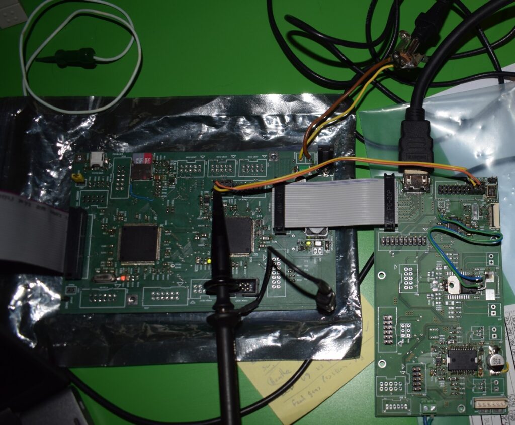
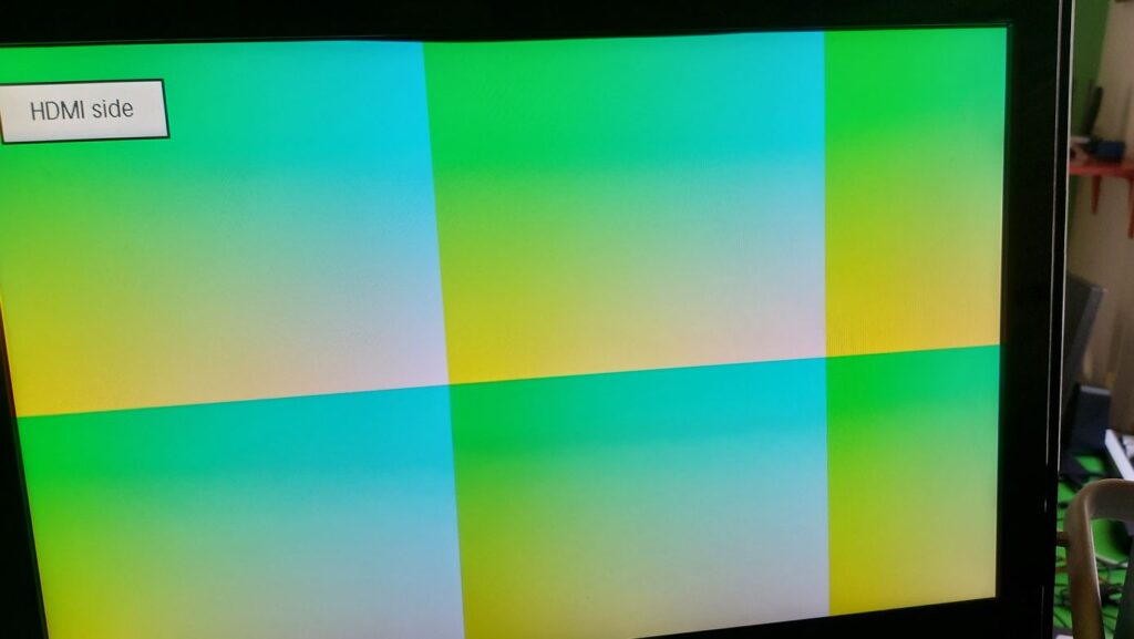
Although I expected to fail, I hoped for the best. Everything was wrong. The TMDS signals had to pass a simple flat cable to interconnect the boards. My reference 25MHz clock had to go with wires back to the main board. In order to reduce the effects of the signal integrity, I used a low resolution of 640×480. For simplicity I added a simple pattern generation. The idea if this worked was to replace it with video memory that the microcontroller would write. The bit rate in the data lanes would be 10 times my 25MHz clock giving 250Mbps per lane. This is where the TV shows says: “Don’t do this at home, experiment executed by Experts”. Well I would stick on the first part: “Don’t do this at home”; I see no expert around….
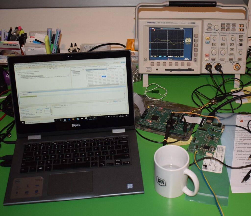
I put my FPGA configuration to my SDCard and modified COFILOS code to load this DVI configuration. I checked that my reference clock was running. My poor 100MHz DPO had not a good chance to capture the high speed data lanes of the serializers outputs.
When my full setup was up an running I connected the HDMI cable… Silence. Excitement. Fear. Waiting to see the result. Nope, needed to select the correct HDMI input at the television. Ok. Let’s see. Oh!
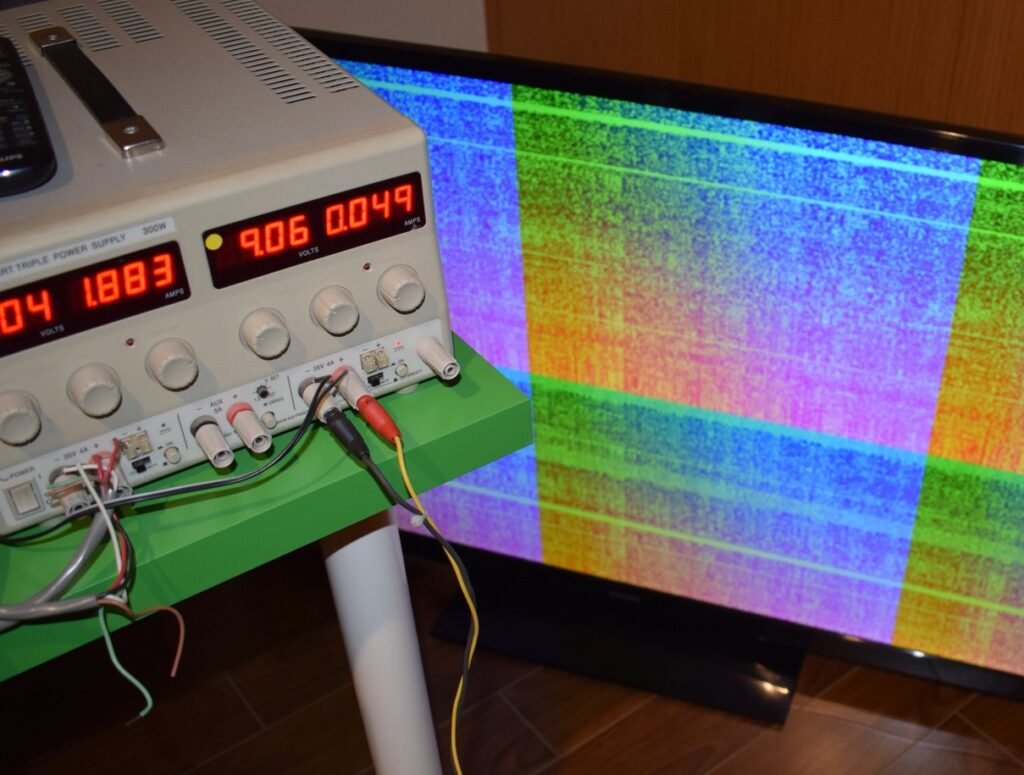
It worked! Well not as it should, but given the circumstances and the implementation I had to follow I am more than happy. The next boards would be tailored to provide proper signal integrity and produce a clean signal.
I did a small redesign in my VHDL to make sure that the issue I was looking, was not related to internal FPGA timings, instead of driving with my test pattern generator I tried driving a constant RGB value. Retrying this on another monitor I had very similar results. I need more specialized hardware to drive it with proper signal integrity and clock signals. No surprise.
At a later time, I also tried to use the internal PLL to generate my clock frequencies. I was not happy with my external 25MHz clock running around. I also did some modifications on my VHDL code as follows .
First I created generics input for the various VESA timings. Now the design is parametric. I also changed the color values to be zero during sync. To reduce timing issues on place and route I also used registered outputs from the Test Pattern Generator.
I started the experiments again with either clock coming from my MCU and create the clock frequencies using the PLL, but still got same results.

As this setup had the same behavior as the original configuration, I reverted to the external 25MHz clock. It seems that this worked after the last changes! I had my DVI output on my monitor. Sometimes tweaking with the HDMI cable could lose the stability of my signal, or maybe the stability of my clock signal going around with cables was not good enough to have a good output, but nevertheless, the proof of concept was completed.
It was really fun to work with SERDES and proprietary vendor IPs and see how they actually work. Really getting into these details provide a good background for other applications.